Photodiode Preamps
- JC - Linear Systems

- Jun 4
- 4 min read
In some JFET op amps such as the AD743, the input capacitance is in the order of 18 to 20 pF. In comparison, with an LSK489 dual FET, the input capacitance is in the order of 3 pF, which will be suitable for low noise photodiode applications. In this section we will see why it is important to have low equivalent input noise and low input capacitance in a photodiode preamp. A simple photodiode is shown in Figure 1 below, which uses an op amp.
In the photodiode amplifier below, when light is shined onto the photodiode, current is generated by the photodiode, PD1. As configured with the cathode of PD1 connected to the (-) input terminal of U1, Vout generates a positive voltage proportional to the amount of light into the photodiode. Also shown in Figure 1 are the equivalent capacitances from the photodiode, Cpd, and (-) input terminal, Cin(-), which are connected in parallel. To minimize Cpd, the photodiode capacitance, the anode of PD1 is connected to the minus 12 volt power supply for maximum reverse bias to lower its junction capacitance. For example, if a BPV10 photodiode is used, Cpd is about 2.7 pF at 12 volts reverse bias. At a lower reverse bias voltage such as 1 volt, Cpd is about 7 pf.
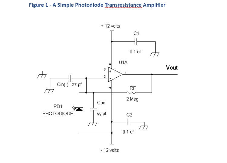
For low noise considerations, these two capacitances, Cpd and Cin(-), should be low as possible. The reason is that the equivalent input noise density voltage, Vnoise_input of the op amp will be amplified in the following manner at Vout, neglecting any noise current from the photodiode:
Vout_noise for a bandwidth of 1 Hz = (Vnoise_input) √(1+(ωRFCt)2 ) + √4kTRF (1)
Where ω = 2πf, RF = feedback resistor, k = 1.38 x10⁻²³ Joules per degrees Kelvin, T = 298 degrees Kelvin
Ct = Cpd||Cin(-) = total capacitance at the (-) input terminal, and
Ct = Cpd + Cin(-)
√4kTRF = thermal noise voltage of the feedback resistor RF for a bandwidth of 1 Hz.
As we can see from the equation above, the output noise, Vout_noise, goes higher if Ct is increased.
In designing a low noise transresistance preamps the goals are to:
Minimum equivalent input noise voltage. Equation (1) above shows that the output noise voltage is dependent on the equivalent input noise voltage, Vnoise_input.
Minimize noise current from the (-) input because the noise current at the input will form a noise voltage across the feedback resistor. Generally, a JFET is desirable for the (-) input because of its low gate noise current.
Minimize the capacitance from the (-) input to ground. The equation (1) shows that more noise is generated at the output when the capacitance, Ct = Cpd + Cin(-), at the (-) input terminal is increased.
Use as large value RF as possible. At first glance, it would appear increasing the resistance in RF would increase the output noise because of the resistor’s thermal noise. This is true but the signal amplification from the photodiode is increased more so that results in a net increase in signal to noise ratio when RF is increased in value. For example, doubling the value in RF increases the resistor noise from RF by √2 = 1.41 while increasing the photodiode signal output voltage by 2. Thus, there is a net gain of √2 or + 3 dB, in terms of signal to noise ratio in this example.
In Figure 1, the typical input capacitance, Cin(-) at the (-) input of an FET op amp is about 18 pf. To lower the capacitance of the op amp, a low capacitance and low noise JFET is used as a buffer or source follower to the (-) input. See Figure 2.
A low noise JFET such as an LSK189 is configured as a source follower, with a source biasing resistor R3. In terms of input capacitance at the gate of J1 with an LSK189, it is about 3 pF from the gate to the drain, which is much less than the 18 pF of Cin(-). Capacitance between the gate and ground due to the gate to source capacitance approaches zero. This is because the source follower configuration provides substantially the same AC voltage at the gate and at the source, which substantially cancels out the capacitance between the gate and the source. The source follower also greatly reduces the capacitance seen at the gate to ground even when the source is driving signal into a capacitive load, Cin(-), the capacitance at the (-) input terminal of the op amp U1A.

It should be noted that the source follower circuit may add some phase shift to the overall amplifier circuit. To ensure phase margin and no oscillations, a resistive divider R1 and R2 is used. With the values given at 3900Ω for R1 and R2, the equivalent feedback resistance is [1 + (R2/R1)] x RF = 2 x 1MΩ = 2MΩ, the same resistance value shown in Figure 1 for RF.
If the (+) input of the op amp in Figure 2 is grounded, such that Voffset = 0 volts, Vout will most likely have a DC offset. To “zero” Vout when there is no signal from the photodiode, a clean DC voltage, Voffset may be applied to the (+) input of U1.
Op amp U1A = AD797 has an equivalent input noise voltage of 0.9 nV/√Hz and J1 =LSK189 with an equivalent input noise voltage of 1.8 nV/√Hz, the total equivalent input noise voltage is about 2.0 nV/√Hz. This is lower than a very low noise JFET op amp such as an AD743 that has 3.2 nV/√Hz. Note that bipolar input stage op amps AD797 with 0.9 nV/√Hz has lower equivalent input noise voltage than 2.0 nV/√Hz, but the AD797’s input noise current is too high and are not suitable for amplifier circuits with large value feedback resistors (RF) in the MΩ such as the circuit shown in Figure 1.
Note that J1 may be substituted with an LSK170 (0.9nV/√Hz ) if a slight increase in capacitance from the gate to ground is acceptable. This FET has about half the equivalent input noise of the LSK189.


Comments